Question
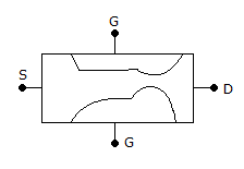
a.
it is the property of material used
b.
the drain end is more reverse biased than source end
c.
drain end is more forward biased than source end
d.
impurity profile changes with distance
Posted under Electronics and Communication Engineering
Interact with the Community - Share Your Thoughts
Uncertain About the Answer? Seek Clarification Here.
Understand the Explanation? Include it Here.
Q. In a biased JFET (Figure) the shape of the channel is as shown because
Similar Questions
Explore Relevant Multiple Choice Questions (MCQs)
Q. In a half wave rectifier, Vrms is
View solution
Q. The approximate value of input impedance of a common emitter amplifier with emitter resistance Re is given by
View solution
Q. The collector voltage VC of the circuit shown in the given figure aside is approximately
View solution
Q. The symbol shown in figure represents a
View solution
Q. Which of the following represents the equivalent circuit of a crystal for crystal oscillator?
View solution
Q. In figure, the function of resistor R is
View solution
Q. The circuit of figure is
View solution
Q. In figure output impedance of amplifier is
View solution
Q. In figure VCEQ for each transistor is
View solution
Q. A multistage amplifier has a low pass response with three real poles at s = - w1 - w2 and w3. The approximate overall bandwidth B of the amplifier will be given by
View solution
Q. In the circuit shown in the figure
View solution
Q. Sweep voltage generators, sweep current generators, multivibrators and blocking oscillators can be combined as
View solution
Q. The configuration of figure is a
View solution
Q. Oscillation frequency in colpitt's oscillator is
View solution
Q. In the case of the circuit shown in the figure Vio = 10 mV dc maximum, the maximum possible output offset voltage Voo caused by the input offset voltage Vio with respect to ground is
View solution
Q. For a sinusoidal input, the circuit shown in the figure will act as a
View solution
Q. The circuit of figure is called
View solution
Q. In figure the potential of gate terminal is
View solution
Q. A distorted sinusoidal has the amplitudes A1, A2, A3 ... of the fundamental, second, harmonic third harmonic, ... respectively. The total harmonic distortion is
View solution
Q. In figure the coordinates of Q point on the load line are (Neglect VBE)
View solution
Recommended Subjects
Are you eager to expand your knowledge beyond Electronics and Communication Engineering? We've handpicked a range of related categories that you might find intriguing.
Click on the categories below to discover a wealth of MCQs and enrich your understanding of various subjects. Happy exploring!