Question
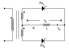
a.
200 V
b.
√2(200) V
c.
√2(400) V
d.
800 V
Posted under Electronics and Communication Engineering
Interact with the Community - Share Your Thoughts
Uncertain About the Answer? Seek Clarification Here.
Understand the Explanation? Include it Here.
Q. In the below figure the rms voltage across each half of secondary is 200 V. The peak inverse voltage across each of thyristor is
Similar Questions
Explore Relevant Multiple Choice Questions (MCQs)
Q. In a single phase full bridge converter (B - 2 connection), the input voltage is v = Vm sin ωt. The output dc voltage for resistive load
View solution
Q. In the below figure, the average value of load current is 15 A. The load is highly inductive. The peak value of thyristor current is
View solution
Q. An n pulse rectifier is fed by a source having an inductance L. If load current is I₀, the voltage drop due to overlap is
View solution
Q. A 3 phase fully controlled bridge converter is fed by a 3 phase system having phase voltage v = Vm sin ωt. The firing angle is a. The dc output voltage is
View solution
Q. In the circuit of figure, the load current when thyristor is off
View solution
Q. In a step down chopper using time ratio control, the input voltage is V and duty cycle is α. The load is purely resistive having resistance R. The average and rms load currents are
View solution
Q. The symbol in figure is for
View solution
Q. If a step down chopper is fed by a dc voltage V with Ton and Toff are on and off periods then following is
View solution
Q. In the circuit of figure, the waveshape of load current when thyristor conducting is
View solution
Q. In figure, thyristor Th is in off state. When thyristor is turned on, the peak thyristor current can be
View solution
Q. In a single phase full wave converter (M-2 connection) feeding on R-L load the input voltage is v = Vm sin ωt. The expression for rms output voltage is
View solution
Q. A dc chopper is feeding an RLE load. The condition for maximum ripple is
View solution
Q. The symbol in figure is for
View solution
Q. The circuit in figure is for
View solution
Q. The symbol in figure is for
View solution
Q. The turn on characteristics of a power transistor can be assumed to be linear, as shown in the below figure . During turn on time T, voltage reduces linearly from V to 0 and current rises linearly from 0 to I. The energy loss during time T is
View solution
Q. The circuit in figure is for
View solution
Q. If 0.5 T is the time period of oscillations and Toff is the time between turn off of one thyristor and turn on of second thyristor, the frequency of output f of a series inverter is
View solution
Q. In auxiliary commutated chopper fed by voltage V and having L and C commutating elements, the peak value of capacitor current is
View solution
Q. A single phase half wave converter is feeding-a resistor load. The input voltage is v = Vm sin ωt. If firing angle is zero, the output dc voltage Vdc and output rms voltage Vrms respectively
View solution
Recommended Subjects
Are you eager to expand your knowledge beyond Electronics and Communication Engineering? We've handpicked a range of related categories that you might find intriguing.
Click on the categories below to discover a wealth of MCQs and enrich your understanding of various subjects. Happy exploring!