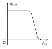
Question

a.
an N MOS inverter with enhanced mode transistor as load
b.
an N MOS inverter with depletion mode transistor as load
c.
a CMOS inverter
d.
BJT inverter
Posted under Electronics and Communication Engineering
Interact with the Community - Share Your Thoughts
Uncertain About the Answer? Seek Clarification Here.
Understand the Explanation? Include it Here.
Q. Given figure is the voltage transfer characteristic of
Similar Questions
Explore Relevant Multiple Choice Questions (MCQs)
Q. An 8-bit microprocessor has 16 bit address bus A₀ - A₁₅. The processor addresses a 1-K byte memory chip as shown. The address range for the chip is
View solution
Q. The circuit shown in the figure is a
View solution
Q. For the circuit shown in the figure, what is the frequency of the output Q?
View solution
Q. Figure shows three pulse train inputs to a 3-input OR gate. Assuming positive logic, the output pulse rate train in figure (b) would be
View solution
Q. For the switch circuit, taking open as 0 and closed as 1, the expression for the circuit is Y. Y is given by
View solution
Q. If number of bits is N, the % resolution in analog to digital conversion is
View solution
Q. Examine the following truth table. The product of sum from this truth table is
View solution
Q. The circuit shown in figure converts
View solution
Q. What is the direction of address bus?
View solution
Q. The logic circuit of the given figure realizes the function
View solution
Q. For the given truth table, the correct Boolean expression is
View solution
Q. The generic microprocessor contains a zero and a carry flag. These are located on the
The 8156 of a figure has RAM locations from 2000 H to 20 FFH.
View solution
Q. The open collector gates in the given figure are tied together. The output Y =
View solution
Q. The dual of the function A(B̅C + BC + BC̅) is
View solution
Q. For the shaded area in Venn diagram of the given figure, the Boolean expression is
View solution
Q. What is the direction of control bus?
View solution
Q. How many zone bits are there?
The 8156 of a figure has RAM locations from 2000 H to 20 FFH.
View solution
Q. The contents of stack location 2109 H after the call operation will be
View solution
Q. For the logic circuit shown in figure, the simplified Boolean expression for the output Y is
View solution
Q. In the given figure assume that initially Q = 1 with Clock Pulses being given, the subsequent states of Q will be
View solution
Recommended Subjects
Are you eager to expand your knowledge beyond Electronics and Communication Engineering? We've handpicked a range of related categories that you might find intriguing.
Click on the categories below to discover a wealth of MCQs and enrich your understanding of various subjects. Happy exploring!


