Question
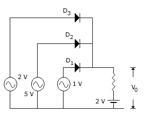
a.
D3, 1 V
b.
D1, 2 V
c.
D2, 5 V
d.
D1, 5 V
Posted under Electronics and Communication Engineering
Interact with the Community - Share Your Thoughts
Uncertain About the Answer? Seek Clarification Here.
Understand the Explanation? Include it Here.
Q. In figure which diode will conduct and what will be the value of V0?
Similar Questions
Explore Relevant Multiple Choice Questions (MCQs)
Q. For the amplifier circuit of figure, the h parameters of transistor are hib = 25 Ω, hfb = 0.999, hob = 10¯⁶ Ω. The voltage gain is
View solution
Q. In figure, VCC = + 30 V, R1 = 200 kΩ and R2 = 100 kΩ. If VBE = 0.7 V, the voltage a cross RE =
View solution
Q. The Vo of the op-amp circuit shown in the given is
View solution
Q. In figure base current is 10 μA and βdc = 100. Then VE =
View solution
Q. In the figure, assume the op-amp is to be ideal. The output Vo if the circuit is
View solution
Q. Assuming VCE sat = 0.2 V and β = 50, the minimum base current (IB) required to drive the transistor in the given figure to saturation is
View solution
Q. In the op-amp circuit given in the figure, the load current iL is
View solution
Q. In figure, secondary winding has 40 turns. For maximum power transformer to 2 ohm resistance the number of turns in primary is
View solution
Q. In figure if the transistor is cut off, the collector voltage is equal to
View solution
Q. In figure, D1 turns on when
View solution
Q. In the circuit of figure both diodes are ideal. If v1 = 10 V and v2 = 10 V which diode will conduct?
View solution
Q. In the circuit of the given figure, assume that the diodes are ideal and the meter is an average indicating ammeter, the ammeter will read
View solution
Q. In the following figure C = 0.02 μF, and Vth is known to be of frequency ω = 10⁷ rad/sec and rd = 2.5 Ω and ZTh = RTh = 10 Ω Then phase angle between id and Vd
View solution
Q. In figure the cut in voltage of diode is 0.7 V and its bulk resistance is 20 Ω. The peak value of circuit current of during positive and negative half cycles are
View solution
Q. In figure, VG =
View solution
Q. In figure the voltage drop across diode is 0.7 V. Then the voltage across diode during negative half cycle is
View solution
Q. In figure vi = 10 mV dc maximum. The maximum possible dc output offset voltage is
View solution
Q. For the circuit of figure the critical frequency is
View solution
Q. The current through R1 is(If β = 99, VBE = 0.74 V)
View solution
Q. The feedback technique employed in the following circuit is
View solution
Recommended Subjects
Are you eager to expand your knowledge beyond Electronics and Communication Engineering? We've handpicked a range of related categories that you might find intriguing.
Click on the categories below to discover a wealth of MCQs and enrich your understanding of various subjects. Happy exploring!