Question
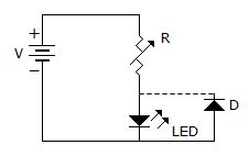
a.
to limit the current and to protect LED against over voltage
b.
to limit the voltage and to protect LED against over current
c.
to limit the current and protect LED against reverse breakdown voltage
d.
none of the above
Posted under Electronics and Communication Engineering
Interact with the Community - Share Your Thoughts
Uncertain About the Answer? Seek Clarification Here.
Understand the Explanation? Include it Here.
Q. In the circuit of figure the function of resistor R and diode D are
Similar Questions
Explore Relevant Multiple Choice Questions (MCQs)
Q. The v-i characteristics of a FET is shown in figure. In which region is the device biased for small signal amplification.
View solution
Q. From the given circuit below, we can conclude that.
View solution
Q. Two identical silicon diodes D1 and D2 are connected back to back shown in figure. The reverse saturation current Is of each diode is 10¯⁸ amps and the breakdown voltage VBr is 50 v. Evaluate the voltages VD1 and VD2 dropped across the diodes D1 and D2 assuming KT/q to be 25 m V.
View solution
Q. As per Einstein's equation, the velocity of emitted electron in photoelectric emission is given by the equation
View solution
Q. Discrete transistors T1 and T2 having maximum collector current rating of 0.75 amp are connected in parallel as shown in the figure, this combination is treated as a single transistor to carry a total current of 1 ampere, when biased with self bias circuit. When the circuit is switched on, T1 draws 0.55 amps and T2 draws 0.45 amps. If the supply is kept on continuously, ultimately it is very likely that
View solution
Q. In given figure a silicon diode is carrying a constant current of 1 mA. When the temperature of the diode is 20°C, VD is found to be 700 mV. If the temperature rises to 40°C, VD becomes approximately equal to
View solution
Q. The current through a PN Junction diode with v volts applied to the P region to the N region, where (I₀ is the reverse saturation current to the diode, m the ideality factor, k the Boltzmann constant, T the absolute temperature and q the magnitude of charge on an electron) is
View solution
Q. In a P-type semiconductor, the conductivity due to holes (= σP) is equal to e = charge of hole, μP = hole mobility, P = hole concentration,
View solution
Q. The collector to emitter cutoff current (ICE0) of a transmitter is related to collector to base cut off current (ICB0) as
View solution
Q. Figure represents a
View solution
Q. In the figure shows the circuits symbol of
View solution
Q. The 6 V zener diode shown in figure has zero zener resistance and a knee current of 5 mA. The minimum value of R, so that the voltage across it does not fall below 6 V is
View solution
Q. For bipolar transistor
View solution
Q. Figure shows characteristics curves for bipolar transistor. These curves are
View solution
Q. In photo electric emission, the threshold frequency f0, work function Uw, and Planck's constant h are related as
View solution
Q. Figure represents a
View solution
Q. The v-i characteristic of an element is shown in below figure the element is
View solution
Q. Diffusion constants Dp, Dn mobility μp, μn and absolute temperature T are related as
View solution
Q. The fT of a BJT is related to its gm, Cπ and Cμ as follows.
View solution
Q. Figure represents a
View solution
Recommended Subjects
Are you eager to expand your knowledge beyond Electronics and Communication Engineering? We've handpicked a range of related categories that you might find intriguing.
Click on the categories below to discover a wealth of MCQs and enrich your understanding of various subjects. Happy exploring!