Question
a.
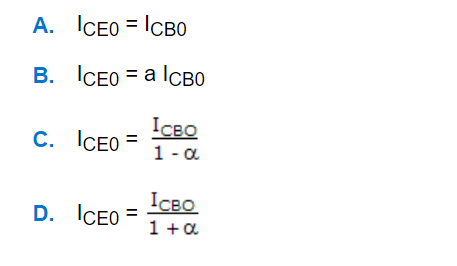
A
b.
B
c.
C
d.
D
Posted under Electronics and Communication Engineering
Interact with the Community - Share Your Thoughts
Uncertain About the Answer? Seek Clarification Here.
Understand the Explanation? Include it Here.
Q. The collector to emitter cutoff current (ICE0) of a transmitter is related to collector to base cut off current (ICB0) as
Similar Questions
Explore Relevant Multiple Choice Questions (MCQs)
Q. Figure represents a
View solution
Q. In the figure shows the circuits symbol of
View solution
Q. The 6 V zener diode shown in figure has zero zener resistance and a knee current of 5 mA. The minimum value of R, so that the voltage across it does not fall below 6 V is
View solution
Q. For bipolar transistor
View solution
Q. Figure shows characteristics curves for bipolar transistor. These curves are
View solution
Q. In photo electric emission, the threshold frequency f0, work function Uw, and Planck's constant h are related as
View solution
Q. Figure represents a
View solution
Q. The v-i characteristic of an element is shown in below figure the element is
View solution
Q. Diffusion constants Dp, Dn mobility μp, μn and absolute temperature T are related as
View solution
Q. The fT of a BJT is related to its gm, Cπ and Cμ as follows.
View solution
Q. Figure represents a
View solution
Q. The O/P char, of a FET is given in the figure. In which region is the device biased for small signal amplification?
View solution
Q. The current in a p-n junction diode with V volts applied in p region relative to n region (where I0 is reverse saturation current, m is ideality factor, k is Boltzmann's constant, T is absolute temp and q is charge on electron) is
View solution
Q. In the BJT amplifier shown in the figure is the transistor is biased in the forward active region. Putting a capacitor across RE will
View solution
Q. Figure shows small signal common base transistor circuit.The current source I and resistor R on the output side are
View solution
Q. The circuit shown in the figure is best described as a
View solution
Q. The current density J, free electron mobility μn, hole mobility μp , magnitude of free electron and hole concentration ni electric field E and charge on electron e, in intrinsic semiconductor are related as
View solution
Q. In bipolar transistors dc current gain is
View solution
Q. Which is correct for a vacuum triode?
View solution
Q. Figure represents a
View solution
Recommended Subjects
Are you eager to expand your knowledge beyond Electronics and Communication Engineering? We've handpicked a range of related categories that you might find intriguing.
Click on the categories below to discover a wealth of MCQs and enrich your understanding of various subjects. Happy exploring!