Question
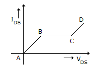
a.
AB
b.
BC
c.
CD
d.
BD
Posted under Electronics and Communication Engineering
Interact with the Community - Share Your Thoughts
Uncertain About the Answer? Seek Clarification Here.
Understand the Explanation? Include it Here.
Q. The O/P char, of a FET is given in the figure. In which region is the device biased for small signal amplification?
Similar Questions
Explore Relevant Multiple Choice Questions (MCQs)
Q. The current in a p-n junction diode with V volts applied in p region relative to n region (where I0 is reverse saturation current, m is ideality factor, k is Boltzmann's constant, T is absolute temp and q is charge on electron) is
View solution
Q. In the BJT amplifier shown in the figure is the transistor is biased in the forward active region. Putting a capacitor across RE will
View solution
Q. Figure shows small signal common base transistor circuit.The current source I and resistor R on the output side are
View solution
Q. The circuit shown in the figure is best described as a
View solution
Q. The current density J, free electron mobility μn, hole mobility μp , magnitude of free electron and hole concentration ni electric field E and charge on electron e, in intrinsic semiconductor are related as
View solution
Q. In bipolar transistors dc current gain is
View solution
Q. Which is correct for a vacuum triode?
View solution
Q. Figure represents a
View solution
Q. To avoid thermal runaway in the design of an analog circuit, the operating point of the BJT should be such that it satisfies the condition.
View solution
Q. Hall coefficient KH and charge density ρ are related as
View solution
Q. In p type semiconductors the conduction due to holes ( = σp ) is (where e = charge on hole, μp is hole mobility and ρ is hole concentration)
View solution
Q. The Ebers-moll equation for IE in CB configuration is given by
View solution
Q. The small signal input impedance of a transistor whose output is shorted for the measuring signal is
View solution
Q. The dipole moment per unit volume as a function of E in the case of an insulator is given by (symbols have the usual meaning).
View solution
Q. The diode and the moving coil milliammeter of figure are assumed to be ideal. The meter reading is
View solution
Q. The V-I characteristic of a semi-conductor diode is shown in figure. From this figure it can be concluded that
View solution
Q. Which of the following expressions may be used to correctly describe the temperature (T) variation of the intrinsic carrier density (ni) of a semiconductor?
View solution
Q. Figure represents a
View solution
Q. Figure shows the terminals of a transistor in plastic package TO 18. Then
View solution
Q. The network shown in the figure represents a
View solution
Recommended Subjects
Are you eager to expand your knowledge beyond Electronics and Communication Engineering? We've handpicked a range of related categories that you might find intriguing.
Click on the categories below to discover a wealth of MCQs and enrich your understanding of various subjects. Happy exploring!
