Question

a.
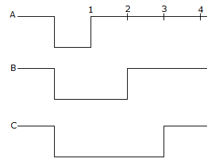
HIGH from 4 to 0
b.
LOW from 0 to 4
c.
HIGH from 0 to 1 and LOW from 1 to 4
d.
LOW from 0 to 2 and HIGH from 2 to 4
Posted under Electronics and Communication Engineering
Interact with the Community - Share Your Thoughts
Uncertain About the Answer? Seek Clarification Here.
Understand the Explanation? Include it Here.
Q. The inputs A, B, C of the given figure are applied to a 3 input NOR gate. The output is
Similar Questions
Explore Relevant Multiple Choice Questions (MCQs)
Q. The circuit of the given figure gives the output Y =
View solution
Q. The number of product terms in the minimized sum of product expression obtained through the following K-map, where d, don't care.
View solution
Q. For the logic circuit of the given figure the simplified Boolean expression is
View solution
Q. In the circuit of the given figure, Y =
View solution
Q. If A = B = 1, the outputs P and Q in the given figure are
View solution
Q. In the given figure, Y =
View solution
Q. The minimized version of logic circuit in the given figure is
View solution
Q. In the given figure shows a negative logic AND gate. If positive logic is used this gate is equivalent to
View solution
Q. The Boolean function/implemented in the figure using two I/P multiplexers is
View solution
Q. For the logic circuit of the given figure the simplified Boolean equation
View solution
Q. In the given figure RC = RL = 1 kΩ, then V0 =
View solution
Q. Inputs A and B of the given figure are applied to a NAND gate. The output is LOW
View solution
Q. For the NMOS gate in the given figure, F =
View solution
Q. The logic circuit of the given figure is equivalent to
View solution
Q. In the given figure shows a logic circuit. The minimum Boolean expression for this circuit is
View solution
Q. The counter shown in the given figure is built using 4 -ve edge triggered toggle FFs. The FF can be set asynchronously when R = 0. The combinational logic required to realize a modulo-13 counter is
View solution
Q. In the figure, the LED
View solution
Q. Four inputs A, B, C, D are fed to a NOR gate. The output of NOR gate is fed to an inverter. The output of inverter is
View solution
Q. The circuit in the figure is has two CMOS-NOR gates. This circuit functions as a
View solution
Q. In the TTL circuit in the figure, S₂ to S₀ are select lines and X₇ to X₀ are input lines. S₀ and X₀ are LSBs. The output Y is
View solution
Recommended Subjects
Are you eager to expand your knowledge beyond Electronics and Communication Engineering? We've handpicked a range of related categories that you might find intriguing.
Click on the categories below to discover a wealth of MCQs and enrich your understanding of various subjects. Happy exploring!


