Question
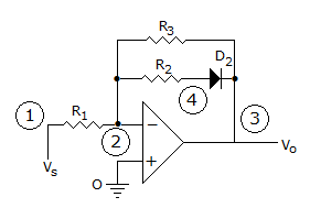
a.
AV = -R3/R1
b.
R3/R1
c.
R1/R3
d.
1 + R3/R1
Posted under Electronics and Communication Engineering
Interact with the Community - Share Your Thoughts
Uncertain About the Answer? Seek Clarification Here.
Understand the Explanation? Include it Here.
Q. Following figure is a signal conditioning Amplifier, changes gain depending upon the polarity of Vs. What will be circuit voltage gain for + Vs and for - Vs if D2 is ideal.
Similar Questions
Explore Relevant Multiple Choice Questions (MCQs)
Q. The circuit of the figure is an example of feedback of the following type
View solution
Q. Oscillation frequency in Wein bridge oscillator is
View solution
Q. In figure VCC = + 30 V, IC corresponding to Q point is 1 mA. If RC = 5 kΩ and RE = 5 kΩ, VCE corresponding to Q point is
View solution
Q. Symbol shown in figure represents a
View solution
Q. In the op-amp circuit of figure, V0 =
View solution
Q. The re model equivalent circuit shown in figure is for
View solution
Q. For the circuit of figure the input and output Miller resistances are
View solution
Q. In the circuit of figure for sinusoidal input the waveform of the output will be as shown in
View solution
Q. In the case of an amplifier, the normalised voltage gain is given by following equation.
where f0 is zero frequency, fP is pole frequency. For a standard frequency response of the amplifier,
View solution
Q. Figure shows a
View solution
Q. In a CC circuit the current gain is
View solution
Q. For the circuit shown in figure low cut-off frequency is
View solution
Q. In the amplifier circuit figure the quiescent point voltage and current are
View solution
Q. For a BJT, β and a are related as
View solution
Q. The circuit diagram shown in the figure consists of transistors in
View solution
Q. The circuit of figure is called
View solution
Q. In the equivalent circuit of figure voltage gain is
View solution
Q. Figure represents a
View solution
Q. In a closed loop non-inverting amplifier, constructed using single break-frequency op-amp, bandwidth with feedback can be written as. (f0 - break frequency, β - gain of the feedback circuit, A - open loop voltage gain, Af - closed loop voltage gain)
View solution
Q. Two identical FETs, each characterised by the parameters gm and rd are connected in parallel. The composite FET is then characterised by the parameters
View solution
Recommended Subjects
Are you eager to expand your knowledge beyond Electronics and Communication Engineering? We've handpicked a range of related categories that you might find intriguing.
Click on the categories below to discover a wealth of MCQs and enrich your understanding of various subjects. Happy exploring!